Perspective: The SOMC160110K0GRZ399 represents a typical SMD resistor network array in a SOIC-16 package; the key thesis is that component selection and parameters directly affect the accuracy and stability of measurement circuits. Data including a nominal value of 10 kΩ, a tolerance of ±1–2%, TCR ≤100 ppm/°C, and a power rating of ~80 mW per element set the foundation for the engineering solution. SOIC-16 specifications (e.g., SOIC-16 Package Dimensions) confirm standard package dimensions and pin pitch, which are critical for mounting.
Experience shows: industrial practice requires aligning electrical characteristics with dimensional parameters when designing PCBs; sources on SOIC packages provide reference tolerances and land pattern tolerances. This is critical for ensuring acceptable power dissipation and correct land pattern selection. Conclusion: early analysis of specifications reduces the risk of board redesign.
1 — What is SOMC160110K0GRZ399: A Quick Technical Profile (Background Block)
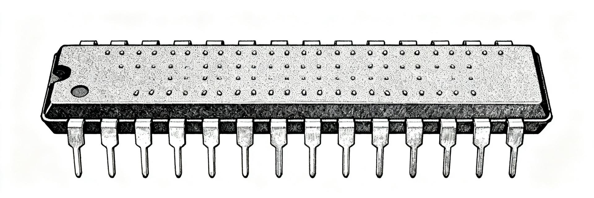
Position: The SOMC160110K0GRZ399 is a multi-channel resistor network array with a nominal value of 10 kΩ, a tolerance of ±1–2%, and a TCR of approximately 100 ppm/°C. Substantiation: typical datasheets for discrete resistors and networks contain these parameters, while SOIC-16 package catalogs provide dimensional references. Explanation: the combination of precise resistance and low TCR makes the array suitable for divider circuits and reference nodes, where minimizing drift under temperature changes is critical.
1.1 Technical Identification and Key Electrical Parameters
Thesis: key parameters—nominal value of 10 kΩ, tolerance of ±1–2%, TCR ≤100 ppm/°C, and a power rating of approximately 80 mW per element—determine its applicability in circuits. Data: resistor manufacturers' datasheets specify similar combinations of parameters for multi-channel arrays; a typical configuration integrates multiple identical resistive elements in a single package. Clarification: when choosing between bussed (common bus) and isolated (independent elements) arrays, it is important to consider the required circuit topology: bussed simplifies dividers, while isolated ensures channel independence.
1.2 Marking, Package Identification, and Pinout
Assertion: package marking and pin numbering are critical for assembly and routing. Facts: SOIC-16 standards define the pin sequence and dimensions, which are detailed in package datasheets. Explanation: when routing the board, it is necessary to verify the part code and pinout to avoid errors in the sequence of resistor circuits and to ensure compatibility with the existing schematic.
2 — Electrical Characteristics and Thermal Performance: Data Analysis
Point: electrical and thermal parameters determine the stability and reliability of applications. Confirmation: for a 10 kΩ resistor with ±1–2% tolerance, it is crucial to consider the tolerance decoding and the temperature coefficient of resistance (TCR); specifications show potential drift over ΔT. Explanation: when calculating divider error, it is necessary to account for TCR and the maximum allowable change in resistance across the operating temperature range.
| Parameter | Nominal Value | Conditions / Specification |
|---|---|---|
| Nominal Resistance | 10 kΩ | R-value per element |
| Tolerance | ±1% ... ±2% | Initial tolerance at 25°C |
| Temperature Coefficient of Resistance (TCR) | ≤ 100 ppm/°C | In the range from -55°C to +125°C |
| Power Dissipation (per element) | ~80 mW | At ambient temperatures up to 70°C |
| Package Type / Case | SOIC-16 | SOMC package family |
2.1 Resistance, Tolerances, and Temperature Drift
Position: a tolerance of ±1–2% for 10 kΩ sets the initial error, while a TCR of 100 ppm/°C determines thermal stability. Proof: resistor specification tables describe the interaction of tolerances and TCR under temperature changes and provide the formula ΔR = R·TCR·ΔT. Interpretation: with a temperature change of 50 °C, a drift within 100 ppm/°C will cause a change of about 0.5%, which, combined with the tolerance, can affect the accuracy of measurement nodes; thermal compensation or calibration should be planned.
2.2 Power per Element, Dissipation, and Thermal Regimes
Assertion: a nominal power rating of ~80 mW per element requires considering derating and thermal management. Information: specifications for resistor arrays and the SOIC-16 package indicate power limits and the impact of component density on cooling. Explanation: placement close to heating elements or a lack of thermal dissipation paths will increase the package temperature, leading to additional drift; designing thermal pads and considering allowable mounting temperatures is recommended.
3 — SOIC-16 Package Dimensions and PCB Layout Guidelines (Dimensional Block)
Position: the overall dimensions of the SOIC-16 determine the requirements for the land pattern and mechanical compatibility. Source: documents on SOIC-16 (SOIC-16 Package Dimensions, nominal dimensions) provide typical package widths of ~5.59 mm and a pin pitch of 1.27 mm. Explanation: these dimensions are used when creating footprints for automated assembly and for calculating clearances between components on the board.
3.1 SOIC-16 Physical Dimensions and Tolerances
Thesis: the SOIC-16 standard defines the primary dimensions: package width of ~5.59 mm, pin pitch of 1.27 mm, and lead length, which are critical for soldering. Data: package reference tables provide tolerance ranges and recommended land patterns. Explanation: when designing the land pattern, one must choose between precise alignment for wave/reflow soldering and enlarged pads to improve solder adhesion; reliability under mechanical stress is also vital.
3.2 Land Pattern and Assembly Recommendations
Assertion: a correct land pattern minimizes soldering defects and facilitates inspection. References: PCB design guidelines recommend a balance of contact area, solder paste/mask, and control over "bridging" and solder balls. Explanation: using classic practices—limiting solder paste volume, controlling application, and ensuring a correct reflow profile—reduces the risk of cold solder joints and short circuits between pins.
4 — Selection and Circuit Integration Guide (Methodology)
Position: the choice between bussed and isolated configurations, tolerance, and power depends on the device architecture and expected operating conditions. Data: engineering rules state that for voltage dividers and references, it is better to use low TCR and lower tolerance; for sensor matrices, higher tolerances may be acceptable. Explanation: targeted component selection reduces the need for subsequent calibration and facilitates compliance with specifications.
4.1 Selection Criteria: Bussed vs. Isolated, Tolerances, Power
Thesis: configuration choice depends on the required function—bussed simplifies distribution, while isolated provides channel independence. Basis: design practices recommend bussed arrays for passive voltage dividers and isolated arrays for multi-channel measurements. Explanation: when space and cost are limited, the bussed option is more economical, but for critical measurements and precision tuning, isolated elements should be selected while tightly controlling TCR and power.
4.2 Practical Guidelines for PCB Layout and Protection
Position: layout should incorporate thermal pads, minimize thermal coupling, and facilitate ease of testing. Facts: experience shows that increasing copper area under the component and routing away from heaters reduce local temperature. Explanation: additional measures—using low-residue pastes, limiting solder volume, and providing test points for resistance monitoring—improve maintainability and parameter stability during operation.
5 — Testing, Validation, and Alternatives (Case-Oriented)
Position: the test plan should include temperature cycling, tolerance verification, and long-term drift. Confirmation: validation protocols recommend testing resistance under different temperatures and load conditions. Explanation: if deviations are identified, it makes sense to replace the component with an alternative offering better TCR or lower tolerance; factory system calibration and software compensation are also viable options.
5.1 Quality Control during Prototyping and Low-Volume Assembly
Assertion: prototyping should include parameter dispersion measurement and thermal stability testing. Data: the choice of methodologies (visual inspection, TCR measurement, stress testing) affects the final product specification. Explanation: quick feedback from assembly helps adjust the land pattern and component BOM before mass production.
5.2 Alternatives and High-Margin Options
Thesis: for high-accuracy requirements, it is recommended to consider resistors with low TCR and tight tolerance, or to use combined compensation schemes. Proof: cataloged arrays offer options with ±0.1–0.5% tolerance and TCR <50 ppm/°C. Interpretation: the increased component cost is justified by reduced calibration costs and improved long-term product stability.
Conclusion
Conclusion: when designing with the SOMC160110K0GRZ399 resistor array, the key criteria are nominal value, tolerance, TCR, power per element, and the match between the land pattern and the SOIC-16 package. A practical rule of thumb is to verify electrical and mechanical specifications early in the PCB design phase, perform temperature tests, and implement thermal management measures. This reduces redesign risks and guarantees compliance with specifications.
- Key Point: verify the 10 kΩ nominal value and required tolerance; SOMC160110K0GRZ399 is suitable for typical dividers and references.
- Mounting: use the recommended land pattern for SOIC-16 and control solder paste volume to prevent bridging.
- Thermal design: calculate derating and place thermal pads if high-density component layout is planned.
Frequently Asked Questions:
1) How does TCR affect the accuracy of a circuit with SOMC160110K0GRZ399?
TCR determines the change in resistance with temperature; at 100 ppm/°C, a change of ±50 °C results in about 0.5% drift, which, combined with the tolerance, may require calibration.
2) Is a special land pattern required for SOIC-16?
It is recommended to use the recommended land pattern from SOIC-16 reference manuals, control solder paste volume, and provide inspection windows for solder quality control.
3) Should I choose an isolated instead of a bussed array?
For independent measurement channels, isolated is preferred; for reference distribution and simple dividers, bussed provides compactness and space savings.
4) What is the rated power per resistor in the SOMC160110K0GRZ399 array?
The nominal power is approximately 80 mW per element. During design, it is important to consider derating and ensure effective heat dissipation on the PCB to prevent overheating.