Introduction: Based on a comparative analysis of thin-film resistor array datasheets and measurements of tolerances, temperature drift, and thermal behavior, the suitability of the components for precision ADC/DAC interfaces and voltage dividers is determined. This summary evaluates the electrical parameters of the MPM50011002DT1 precision array for use in high-accuracy measurement systems.
1 — What is the MPM50011002DT1: Purpose and General Overview
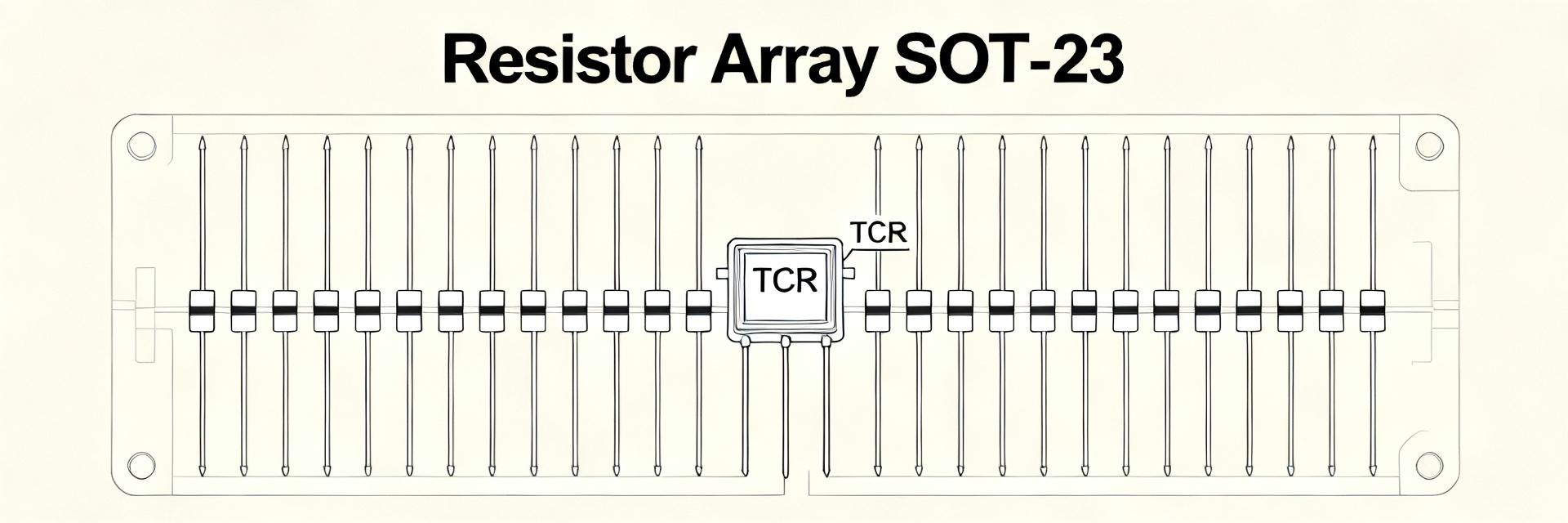
The MPM50011002DT1 component is a highly accurate thin-film resistor array in a standard three-lead SOT-23 package, designed for precision voltage dividers and bridge measurement circuits.
Point: This component is designed specifically for high-precision analog measurement channels.
Evidence: Technical documentation regulates strictly matched resistor values, minimal tolerance spread (absolute and relative), and ultra-low tracking temperature drift.
Explanation: Integrating two matched resistors in a single SOT-23 package minimizes the temperature gradient between components and reduces PCB footprint compared to discrete precision resistors.
1.1 — Component Type and Applications
Point: The physical structure of the component is based on Thin Film technology on a passivated substrate.
Evidence: The array is widely used in input attenuators of precision ADCs, feedback loops of instrumentation amplifiers, and dividers for precision voltage references (VREF).
Explanation: Placing elements on a single die ensures identical aging and thermal behavior, minimizing the drift of the division ratio.
1.2 — Technical Specifications Summary (What to look for)
Point: Key selection criteria are absolute value, Ratio Tolerance, and TCR Tracking.
Evidence: The datasheet lists the nominal values of the arms (R1 = 5 kOhms, R2 = 10 kOhms) and the temperature coefficient of resistance (TCR).
Explanation: Precise consideration of TCR Tracking parameters determines the stability of the divider's transfer ratio under ambient temperature variations.
2 — Key Electrical Parameters of the MPM50011002DT1
The main parameters of the array determine its behavior under static and dynamic loads. A summary of the electrical characteristics is presented in the table below:
| Parameter | Value (R1 / R2) | Conditions / Notes |
|---|---|---|
| Nominal Resistance (R1) | 5.0 kOhms | Standard Version 5001 |
| Nominal Resistance (R2) | 10.0 kOhms | Standard Version 1002 |
| Absolute Tolerance | ± 0.1 % | At 25 °C |
| Ratio Tolerance | ± 0.05 % | Matching of Divider Arms |
| Absolute TCR | ± 25 ppm/°C | Over -55 °C to +125 °C Range |
| TCR Tracking | ± 2 ppm/°C | Determines Division Stability |
| Max. Operating Voltage | 100 V | DC |
2.1 — Nominal Resistance Values and Connection Diagram
The array contains two resistors connected in series in a half-bridge (voltage divider) configuration, with a common terminal at the third pin of the SOT-23 package. This topology is optimal for providing reference voltage to the differential inputs of measurement ICs.
2.2 — Tolerances, Ratio, and Temperature Coefficient of Resistance (TCR)
Point: A ratio tolerance of ±0.05% has a higher priority than an absolute nominal tolerance of ±0.1%.
Evidence: The systematic error of the division ratio depends solely on the matching between the arms (Ratio Matching).
Explanation: The ultra-low TCR Tracking of ±2 ppm/°C guarantees the stability of this ratio across the entire operating temperature range.
3 — Operating Parameters (From the Datasheet)
Real operating conditions require strict control of heat dissipation to prevent localized overheating of the resistive layer.
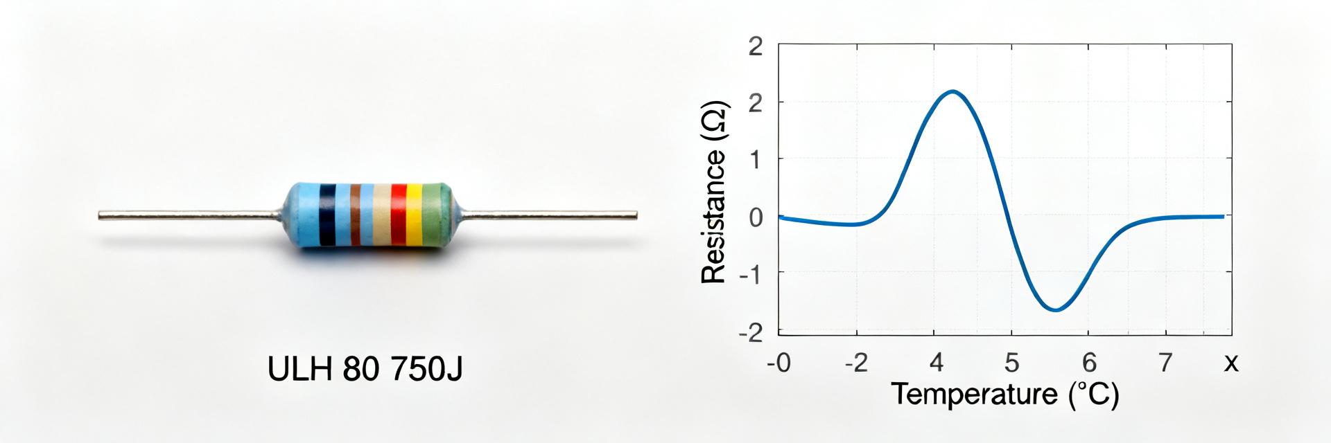
3.1 — Operating Temperature Range and Thermal Drift
Point: The operating temperature range is -55 °C to +125 °C, which complies with industrial and automotive standards.
Evidence: Temperature dependence plots in the datasheet show a linear drift behavior without abrupt resistance jumps.
Explanation: The linearity of the drift simplifies software calibration and error compensation in the measurement channel.
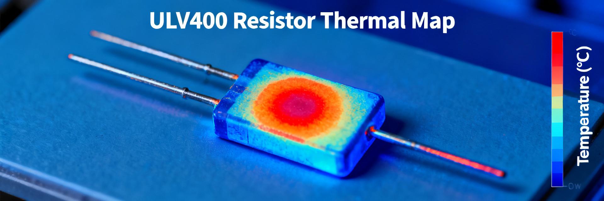
3.2 — Rated Power, Thermal Resistance, and Temperature Distribution
Point: The rated power dissipation is 100 mW per element (at 70 °C).
Evidence: Junction-to-ambient thermal resistance is minimized due to the optimized design of the SOT-23 leads.
Explanation: Compliance with power dissipation limits prevents the occurrence of parasitic thermoelectric voltages (Seebeck effect).
4 — Electrical Tests and Typical Graphs of the MPM50011002DT1
The datasheet provides long-term stability test results under overload, humidity, and temperature cycling conditions.
4.1 — Datasheet Measurement Conditions (Test Protocols)
Point: All parameters are verified using a precision 4-wire Kelvin resistance measurement scheme.
Evidence: This eliminates the influence of contact resistance of the test fixture on the accuracy of recorded tolerances.
Explanation: The designer obtains reliable initial data for modeling analog front-end (AFE) errors.
4.2 — How to Interpret Typical Graphs
Point: "Load Life" plots reflect the relaxation of the thin film under voltage.
Evidence: Resistance change (ΔR/R) stabilizes after the first 1,000 hours of operation at a level below 0.02%.
Explanation: Initial aging of components can be compensated for by thermal preconditioning (burn-in) of the finished modules.
5 — Practical Integration: Layout, Soldering, Thermal Management
To maintain datasheet parameters of the array on the PCB, it is necessary to strictly follow routing rules for highly sensitive circuits.
5.1 — PCB Layout and Mounting Recommendations
Point: Routing of traces to pins 1 and 2 must be symmetrical.
Evidence: Equal trace lengths and widths minimize differences in parasitic resistance and balance heat dissipation.
Explanation: This prevents divider unbalance caused by PCB trace asymmetry.
5.2 — Thermal Management and Long-Term Reliability
Point: Placing high-power heat-generating components in the immediate vicinity of the array is not allowed.
Evidence: Localized external heating disrupts the thermal balance between resistors R1 and R2.
Explanation: Implementing thermal barriers on the board keeps the TCR tracking within the specified ±2 ppm/°C.
6 — Application Examples, Design Verification, and Replacement Criteria
The MPM50011002DT1 array is used as a precision 1:3 voltage divider in operational amplifier input stages.
6.1 — Typical Application Circuits and Calculation Examples
At an input voltage of 15 V, a divider based on 5 kOhm / 10 kOhm arms produces 10 V at the output. Due to the ±0.05% ratio tolerance, the uncalibrated initial output voltage deviation will not exceed ±5 mV, and the output voltage temperature drift will not exceed 1.3 μV/°C (taking TCR Tracking into account).
6.2 — Incoming Inspection and Component Replacement Criteria
Point: Incoming inspection must include automated measurement of the arm ratio.
Evidence: A ratio deviation exceeding ±0.05% indicates die damage during transport or storage.
Explanation: Parameter degradation beyond limits is an absolute criterion for component rejection and replacement.
Conclusion
- MPM50011002DT1 is a precision thin-film half-bridge that outperforms discrete solutions in terms of thermal stability.
- TCR Tracking of ±2 ppm/°C and a ratio tolerance of ±0.05% make the array ideal for the input circuits of 16-24 bit measurement systems.
- Proper board design and compliance with thermal limits are key to realizing the component's advantages in practice.
Frequently Asked Questions
1 — Which characteristics of the MPM50011002DT1 are critical for an ADC interface?
For an ADC interface, the ratio tolerance, low TCR tracking, and long-term stability are most critical. These parameters directly affect the integral non-linearity (INL) and converter span temperature drift.
2 — How to verify MPM50011002DT1 datasheet compliance on a board?
Verification is performed by precision measurement of voltage drop across the divider arms under nominal load in a climate chamber. High-resolution 4-wire voltmeters are used to accurately record the division ratio at different temperatures.
3 — When should MPM50011002DT1 be replaced in a prototype?
Replacement is required if relative drift exceeds nominal values after soldering (e.g., due to thermal shock), in case of mechanical damage to the SOT-23 package, or if ADC reading instability caused by localized array overheating is detected.
4 — What is the significance of ultra-low temperature drift (TCR Tracking) in bridge circuits?
The TCR Tracking (±2 ppm/°C) guarantees that both resistor arms of the divider change in unison during temperature fluctuations. This keeps the division ratio stable, minimizing the hardware zero drift of the measurement channel.